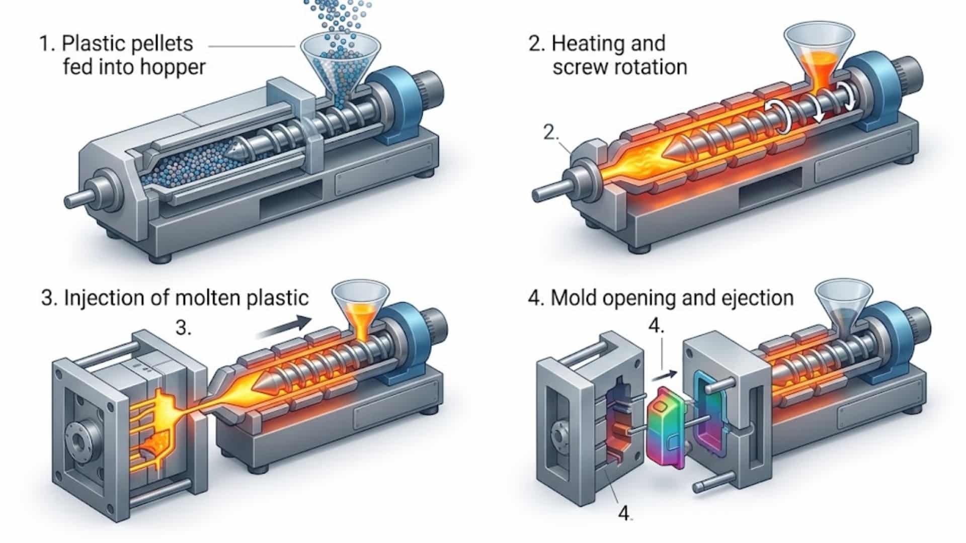

Scaling a consumer electronic product from initial CAD rendering to mass production requires balancing exterior cosmetics, internal structural integrity, and tight assembly tolerances. Precision injection molding for consumer products bridges the gap between industrial design intent and cost-effective, high-volume manufacturing.
Successfully launching electronic housings and structural internal components depends on three core decisions: selecting resins that balance drop impact resistance with flame-retardant standards, designing tooling that mitigates thin-wall flow defects, and vetting an OEM manufacturing partner equipped with multi-axis quality verification and intellectual property protection protocols. This engineering guide breaks down the resin selection criteria, DFM (Design for Manufacturability) guidelines, tooling roadmaps, and quality control systems required for consumer electronic applications.
Precision Injection Molding for Consumer Electronics: Balancing Aesthetics, Tolerances, and Speed-to-Market
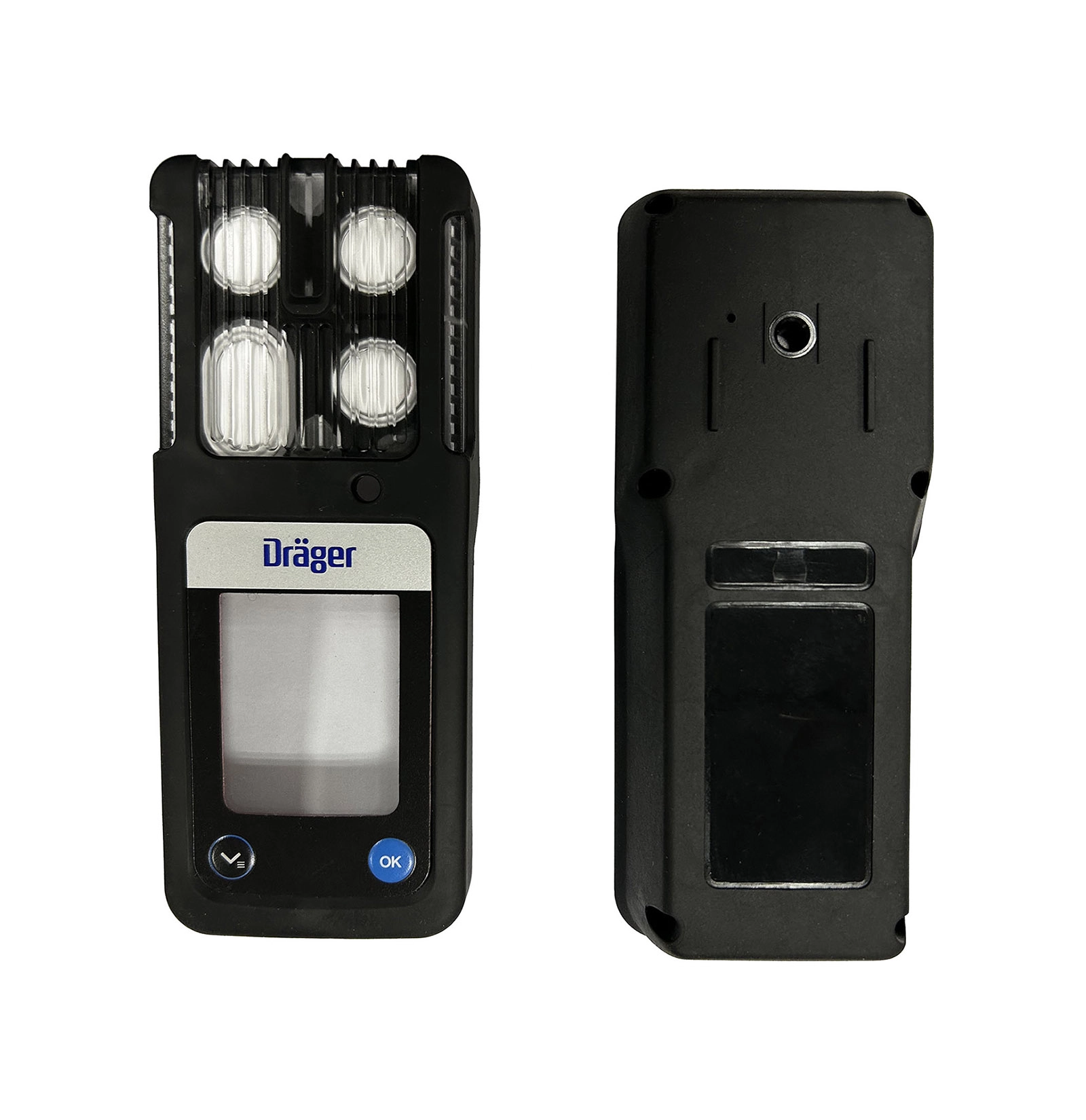
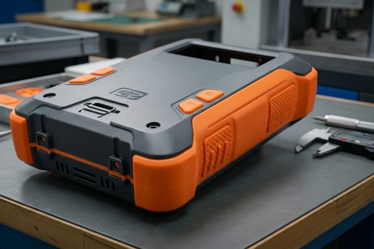
Consumer electronic devices—such as smart home hubs, wearables, audio gear, and handheld peripherals—face a unique dual constraint: they require Class-A cosmetic surfaces alongside intricate internal mechanical geometries.
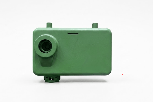
Consumer Electronic Molding Duality
| Aesthetic Requirements | Functional Tolerances |
|---|---|
| High-gloss / textured finishes | Micro-snap fits & living hinges |
| Zero sink marks over thick ribs | Thin-wall flow (sub-1.0 mm) |
| Invisible weld and knit lines | PCB retention boss alignments |
| Consistent colorant batching | Ingress protection (IP) sealing |
Achieving structural rigidity without adding excessive wall thickness requires high-precision tooling and precise melt-flow control. For mechanical designers and procurement engineers, working with a partner specializing in custom plastic injection molding ensures that cosmetic demands do not compromise mechanical snap fits, screw bosses, or ingress protection (IP) sealing channels.
Engineering Plastics Selection: Material Properties vs. Functional Demands
Selecting the right polymer matrix dictates thermal resistance, impact attenuation, surface finish, and wireless signal transparency.
Common Thermoplastics: ABS, PC, PC/ABS Blends, and Specialty Resins
- ABS (Acrylonitrile Butadiene Styrene): Offers excellent dimensional stability, ease of electroplating/painting, and superior processability. Commonly selected for cost-sensitive handheld housings where moderate impact resistance is sufficient.
- PC (Polycarbonate): High mechanical toughness, optical clarity, and elevated heat deflection temperatures (HDT). Ideal for transparent display windows, light pipes, and impact-critical outer shells, though it exhibits higher melt viscosity.
- PC/ABS Blends: Combines the thermal and impact performance of PC with the melt flow and cosmetic surface fidelity of ABS. Widely used for structural electronic housing injection molding requiring UL94-V0 flame retardancy and drop-test survival.
- PMMA (Acrylic): Exceptional light transmission and UV resistance for scratch-resistant optical lenses and external capacitive touch panels.
- Polyamides (Nylon / PA + Glass Fiber): Chosen for internal skeletal frames, antenna brackets, and sub-chassis where high stiffness and minimal creep are required.
Consumer Electronics Material Selection Matrix
| Resin Type | Mechanical Toughness | Cosmetic / Surface Capability | Processing & Shrinkage Profile | Typical Applications |
|---|---|---|---|---|
| ABS | Moderate | High (Accepts texture, gloss, paint) | Uniform shrinkage (~0.4–0.7%), easy flow | Remote controls, smart speaker bases |
| PC | Exceptional | High (High gloss, optical clear) | Lower flow rate, higher internal stress | Display lenses, rugged device shells |
| PC/ABS Blend | High | Superior (Resists knit line visibility) | Balanced shrinkage (~0.5–0.7%), good flow | Laptop chassis, monitor housings, POS terminals |
| PMMA | Low (Brittle) | Exceptional (Optical grade) | Sensitive to packing pressure and moisture | LED diffusers, indicator covers |
| PA + 30% GF | Very High | Low to Moderate (Fiber print-through) | Anisotropic shrinkage, abrasive to tooling | Internal structural chassis, sub-frames |
For non-structural, high-voltage internal components requiring high dielectric isolation and thermal endurance, engineers may evaluate thermoset molding alternatives to maintain geometry under prolonged operational heat.
Advanced Tooling & DFM: Overcoming Molding Defects in Electronic Devices
Tooling design directly dictates part consistency and scrap rates. Addressing flow imbalances during early DFM prevents common cosmetic and functional failures.
DFM Wall Thickness & Rib Proportions (Schematic)
- Nominal Wall (T): Maintain consistency throughout.
- Rib Width (W) = 0.4T to 0.6T (Prevents Sink Marks)
- Rib Height (H) ≤ 3T (Prevents Ejection Sticking)
- Radius (R) = 0.25T to 0.5T (Relieves Stress)
- Draft Angle = 0.5° to 1.5° per side
Critical Design Considerations: Wall Thickness, Ribs, and Gating
- Nominal Wall Uniformity: Maintain constant wall thickness throughout the part. Sudden transitions create localized differential shrinkage, causing dimensional warpage across mating housing halves.
- Rib-to-Wall Proportions: Keep internal stiffening ribs between 40% and 60% of the nominal wall thickness. Ribs exceeding this ratio draw heat away slowly from the adjacent cosmetic surface, creating visible sink marks.
- Gate Type and Placement: Use edge gates, sub-gates, or valve-gated hot runners placed along non-cosmetic part edges or under battery compartments. Proper gate positioning prevents weld lines from forming across structural screw bosses or thin display bezels.
- Draft Angles: Apply minimum draft angles of 0.5° to 1.0° on core/cavity shutoffs, increasing to 3.0° to 5.0° on surfaces designated for heavy EDM spark erosion or chemical texturing to prevent drag marks during ejection.
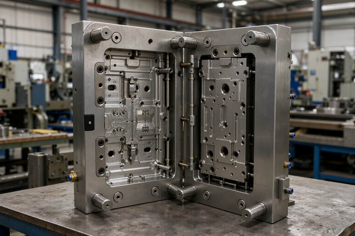
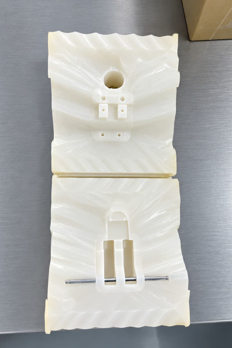
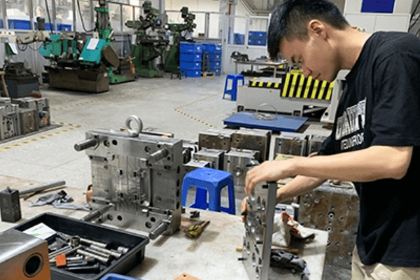
Building durable production tools requires precision plastic mold fabrication using hardened tool steels (such as NAK80, S136, or H13). Complex slide actions, lifters, and interchangeable inserts are typically fabricated via CNC machining to maintain mold shutoff tolerances and prevent flash across multi-part splits.
Scaling Your Product: From Rapid Prototyping to Mass Production
Hardware programs progress through distinct development stages. Aligning the tooling strategy with expected production volumes controls upfront capital expenditure and lead times.
Production Volume & Tooling Roadmap
| EVT / DVT Stage (1 – 100 Parts) | PVT / Pilot Run (100 – 5,000 Parts) | Mass Production (10,000+ Parts) |
|---|---|---|
| 3D Printing | Bridge Tooling | Multi-Cavity Hard Tooling |
| CNC Machining | Aluminum / P20 | Hardened Steel (S136, H13) |
| Vacuum Casting | Fast cycle trials | Hot Runner Systems |
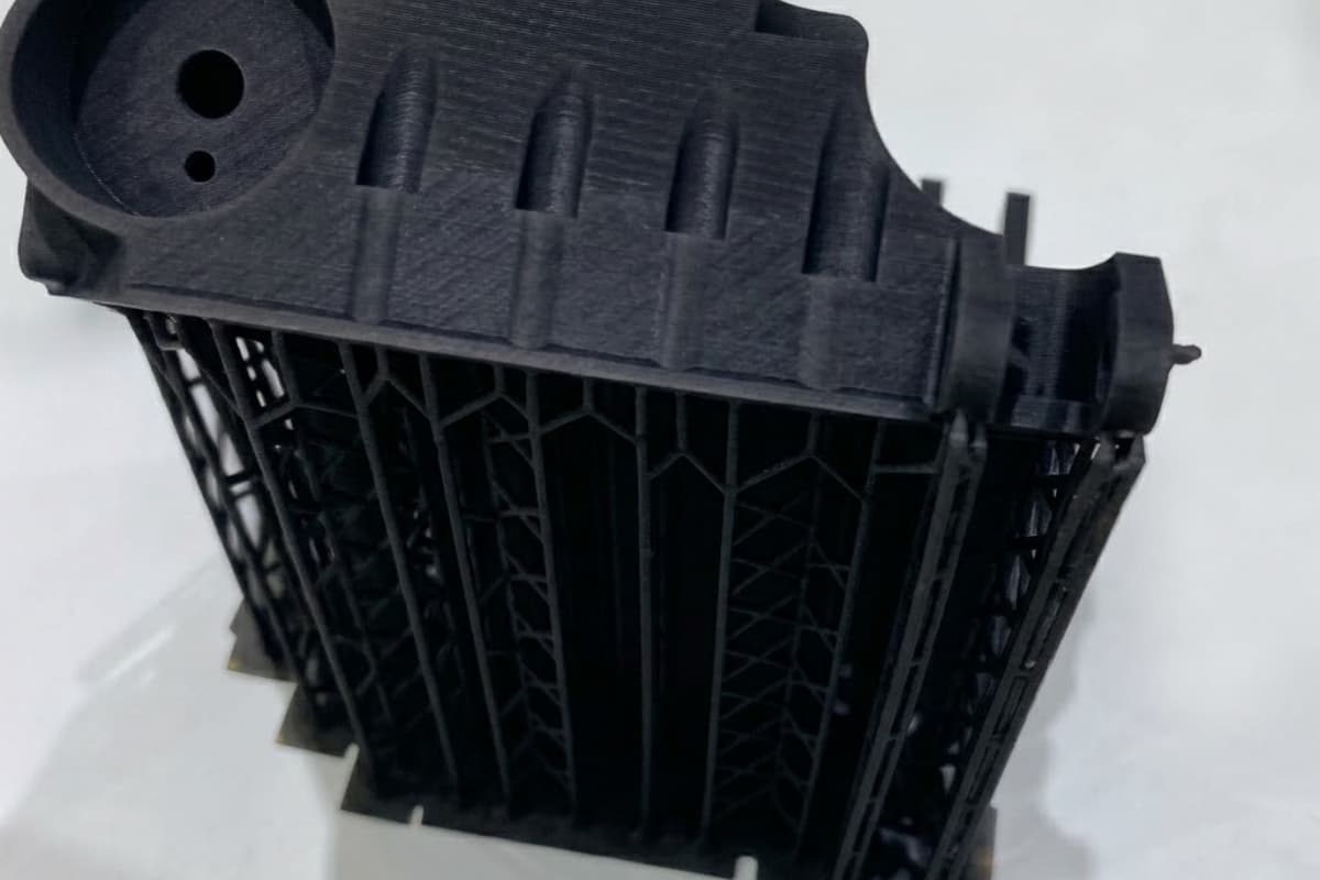
- EVT (Engineering Validation Test): Focuses on geometric fit and PCB alignment. Teams rely on functional rapid prototyping methods or vacuum casting using polyurethane resins that simulate production ABS and PC.
- DVT (Design Validation Test): Validates actual mechanical and thermal performance. Bridge tooling utilizing P20 or aluminum mold cores delivers initial injection-molded parts in the intended engineering resins without the lead times of multi-cavity production tooling.
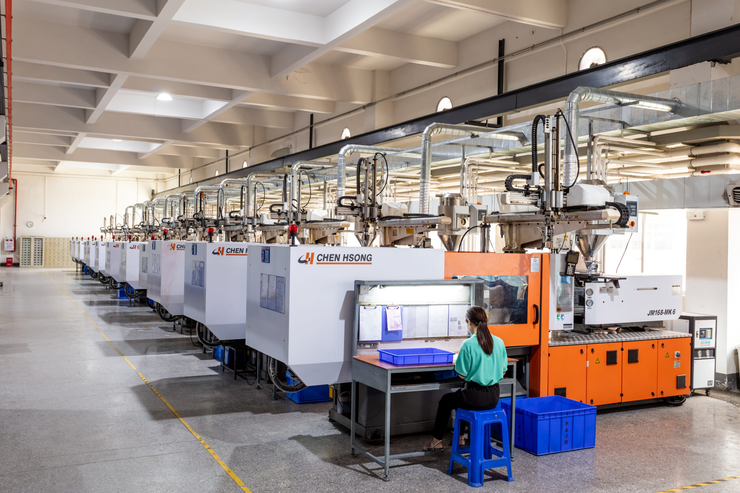
- PVT & Mass Production: Hardened steel molds (such as multi-cavity, fully automated tools) are deployed to optimize cycle times, maintain process repeatability, and lower unit economics. For large enclosures or low-to-mid volume housings with complex geometry, reaction injection molding (RIM) can serve as an alternative to reduce upfront tooling capital.
Ensuring Quality Consistency and Intellectual Property Security in Offshore OEM Partnerships
Sourcing an injection molding OEM manufacturer requires rigorous verification of process capability, dimensional metrology, and data security.
Quality Control and Metrology Framework
To prevent assembly failures on automated surface-mount (SMT) or final box-build lines, production parts must undergo continuous verification:
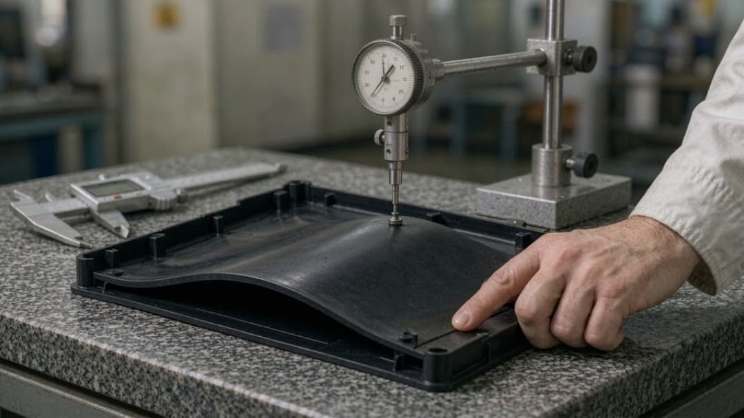
- First Article Inspection (FAI): 100% dimensional verification against critical-to-function (CTF) GD&T drawings using automated coordinate measuring machines (CMM) and optical video measuring systems.
- Process Capability Studies (Cpk / Ppk): Verification that critical dimensions (such as interlock snaps and perimeter gasket grooves) demonstrate Cpk ≥ 1.33 stability across multi-cavity tools.
- Environmental and Fit Testing: Drop testing, thermal cycling, color spectrophotometer evaluation (Delta E), and cross-hatch adhesion testing for coated or printed enclosures.
These verification workflows depend on a structured quality control system supported by certified inspection and metrology equipment.
Intellectual Property & Engineering Collaboration
International original equipment manufacturing requires strong intellectual property management:
- Non-Disclosure Agreements (NDA): Comprehensive bilateral IP protection executed before transferring CAD data, PCB STEP models, or industrial design renders.
- Engineering Change Order (ECO) Management: Formal change-tracking protocols ensuring tool modifications and revision updates are synchronized across CAD files, CAM programs, and physical mold cavities without cross-cultural delays.
- Direct Engineering Support: Clear, cross-border technical communication to resolve DFM challenges and material substitutions without project stalling.
Key Takeaways
- Material Balancing: Match mechanical requirements to the polymer: ABS for general enclosures, PC for impact strength and transparency, and PC/ABS blends for high-reliability consumer electronic housings.
- Proportional Wall Geometry: Prevent visible cosmetic sink marks and warpage by restricting internal rib thickness to 40%–60% of the nominal wall and maintaining consistent wall thickness throughout the part.
- Staged Tooling Strategy: De-risk early hardware builds by utilizing CNC prototyping and bridge tooling during EVT/DVT before investing in multi-cavity, hardened steel production molds.
- Quality & IP Governance: Audit suppliers based on physical CMM metrology capabilities, statistical process control (Cpk), formal ECO workflows, and strict NDA protocols.
Frequently Asked Questions (FAQ)
What is the typical lead time for precision mold fabrication for electronic enclosures?
Lead times vary depending on part complexity, surface finish specifications, and slide/lifter mechanisms. Prototype bridge molds typically take 2 to 3 weeks, while complex, multi-cavity hardened steel production molds generally require 4 to 7 weeks from final DFM sign-off to First Article Inspection (FAI) samples.
Which CAD file formats are best suited for an injection molding DFM review?
Native STEP (.step, .stp) and Parasolid (.x_t) formats are standard for 3D geometric and mold flow evaluations. Supplemental 2D drawings in PDF or DXF format indicating critical-to-function (CTF) dimensions, GD&T tolerances, surface textures (e.g., Mold-Tech standards), and threaded insert callouts are necessary for complete quoting.
How are cosmetic sink marks eliminated above internal screw bosses?
Sink marks are eliminated by coring out the base of thick screw bosses, adding gusset ribs for structural support instead of increasing wall mass, and maintaining a core-to-wall thickness ratio below 60%. Implementing proper pack and hold pressures during the molding cycle further prevents localized material shrinkage.
Contact GoodTech for technical support
Ready to transition your electronic enclosure design into production-ready parts? Submit your STEP files to the engineering team at GoodTech for a confidential DFM evaluation, material mold-flow review, and tooling proposal: Contact GoodTech Engineering.