
Scaling a consumer electronic product from CAD to mass production succeeds or fails on five decisions. First, how you classify the part and define its requirements. Second, which resin you select. Third, the design-for-manufacturability (DFM) rules you lock in before tooling. Fourth, the tooling strategy you choose across development stages. Fifth, how you verify cost and supplier capability. This guide walks through all five in order — moving from your design question to a manufacturing decision — so mechanical engineers, NPI managers, and procurement leads can de-risk an electronics enclosure or structural component program before committing to steel.
Who this is for: consumer-electronics brand engineers, hardware program managers, procurement and supply-chain leads, and founders building their first injection-molded product. How to use it: the sections are independent. Jump to Material Selection if resin is your bottleneck, or Tooling Strategy if you are planning an EVT build. Read straight through if you want the full decision chain.
What Makes Consumer Electronics Injection Molding Different

Consumer electronics parts face a dual constraint that general-purpose molded parts do not. The same component must deliver a Class-A cosmetic surface while also holding micro-snap fits, living hinges, PCB retention bosses, and ingress-protection (IP) seals — often at sub-1.0 mm wall sections. A cosmetic bezel and a structural frame may be the same molded part, yet each demands a different priority.
| Aesthetic Requirements | Functional Tolerances |
|---|---|
| High-gloss / textured finishes | Micro-snap fits & living hinges |
| Zero sink marks over thick ribs | Thin-wall flow (sub-1.0 mm) |
| Invisible weld & knit lines | PCB retention boss alignments |
| Consistent colorant batching | Ingress protection (IP) sealing |
Three consequences separate this work from commodity molding. Thin-wall flow demands precise melt-flow control; any hesitation leaves short shots on display bezels. Cosmetic/mating conflict means a screw boss placed under a visible surface causes sink marks exactly where they cannot appear. RF transparency — plastic passes radio frequency — means every wireless product needs an explicit EMI plan, which we cover in Step 3.
Explore our plastic injection molding capabilities.
Step 1 — Classify Your Part and Define Requirements
Before any CAD detail, classify the molded component by its primary function. A cosmetic bezel, a structural frame, and a flexible button may use the same process but obey different design rules.
- Cosmetic — controls appearance and protects the product.
- Structural — supports loads, fasteners, or mating components.
- Interactive — buttons, keycaps, sliders, battery doors.
- Protective — absorbs impact or blocks access to sensitive areas.
- Flexible — sealing, grip, cushioning, hinge movement.
When one part plays several roles, decide the priority. A housing may need to support screw bosses and keep a clean exterior — and poor boss placement sinks the visible face.
Requirement checklist. Document the use environment before selecting plastic: normal and peak temperature, drop height or handling load, chemical contact (cleaners, oils, cosmetics), UV exposure, expected service life in years or cycles, and whether users open or clean it repeatedly. Set measurable cosmetic standards — mark Class-A surfaces, define acceptable color, gloss, texture, and assembly gaps on the drawing, and restrict where gates, ejector marks, and parting lines may land. Descriptions like “premium feel” are not inspection criteria. Lock production targets — expected annual volume, assembly method (snaps, screws, inserts, welding, adhesive), and critical dimensions — before requesting a manufacturing review.
See our custom injection molding DFM process.
Step 2 — Material Selection: Matching Resin to Product Demands

Material selection must happen before detailed feature design. Resin stiffness drives rib layout; shrinkage drives housing alignment; allowable strain decides whether a snap-fit survives assembly. Final decisions use the exact grade datasheet, not the family average.
| Resin | Toughness | Cosmetic | Shrinkage & processing | Typical use |
|---|---|---|---|---|
| ABS | Moderate | High | Uniform ~0.4–0.7%, easy flow | Remotes, speaker bases |
| PC | Exceptional | High (optical clear) | Lower flow, higher stress | Lenses, rugged shells |
| PC/ABS | High | Superior | Balanced ~0.5–0.7% | Laptop/monitor housings |
| PMMA | Low | Exceptional (optical) | Moisture-sensitive | Diffusers, covers |
| PA + 30% GF | Very high | Low–moderate | Anisotropic, abrasive | Internal chassis |
| PP | Moderate | Moderate | High shrink, good hinge | Hinges, chem-resistant |
| TPE/TPU | Flexible | Soft-touch | Bonding-dependent | Buttons, seals |
Flame retardancy (UL94). Many enclosures require UL94-V0, but a flame-rated resin does not auto-certify the finished product — the rating is grade- and thickness-specific. Confirm the applicable standard, tested thickness, color, and recognized material data; halogen-free FR is increasingly required for EU markets. Shrinkage & stability. Molded plastic shrinks as it cools; the result depends on material, geometry, gate location, fiber orientation, and process, and it shifts seams, buttons, and latches. For moisture-sensitive resins such as PA, state in the inspection spec whether parts are measured dry or after conditioning.
Antenna / RF window. Wireless products need signal clearance at antenna near-field zones. As a design rule, avoid metal inserts, conductive paint, and plating within the antenna near-field and keep those zones in plain RF-transparent plastic. Exact exclusion distances and keep-out geometry must be confirmed with the RF/antenna engineering team for the specific frequency band and module — treat as “to be verified” until specified.
For high-voltage, high-heat internal components, evaluate thermoset molding alternatives.
Step 3 — DFM Design Rules That Decide Success
These are the parameters that separate a clean production run from scrap. Values below are engineering rule-of-thumb ranges; the final call uses the specific resin grade datasheet and a DFM review.
| Parameter | Rule of thumb | Failure if ignored |
|---|---|---|
| Nominal wall | Uniform throughout | Warpage across mating halves |
| Rib width | 40–60% of nominal wall | Sink marks on A-surface |
| Rib height | ≤ 3× nominal wall | Ejection sticking |
| Corner radius | 0.25–0.5× wall | Stress concentration |
| Draft angle | 0.5–1.5° per side | Drag marks on ejection |
| Textured-surface draft | +1° per ~0.025 mm texture | Whitening on textured walls |
Screw bosses. Outer diameter ≈ 2× the screw-hole diameter; keep boss wall in the 40–60% band and use gussets instead of thick bases. Core out the base to kill sink. For any fastener a technician touches more than once, specify brass heat-stake or ultrasonic inserts — a reusable metal thread with no boss cracking — and mold the pilot hole from T1. Self-tapping screws remain defensible only for one-time, extreme-cost-pressure assembly. Snap-fits. Cantilever snap strain must stay below the resin limit (under ~2% for most PC/ABS) so housings assemble tool-free at line speed; design release to avoid side actions where possible, since every lifter and slider adds cost and maintenance to every shot. Gate location. Keep knit lines off cosmetic A-surfaces and away from EMI gasket lands — a knit line on a conductive-coating land creates a coating-thickness discontinuity and a leak point. Submarine gates on hidden edges hide gate marks; run mold-flow simulation at DFM to catch this before steel is cut. Parting line & pull direction. Set the mold-opening direction before the external design is frozen; place the parting line along a natural edge and keep seams away from primary viewing surfaces.
EMI shielding — three routes (decision framework)
| Strategy | How it works | Shielding | Best when |
|---|---|---|---|
| Conductive coating | Cu/Ni/Ag paint or vacuum metallization inside shell | Good (40–80 dB, full coverage) | Mid volumes; complex geometry; localized zones |
| Conductive-filled resin | Stainless/carbon/nickel fiber compounded in resin | Moderate (absorption-dominant) | Very high volumes; repeatability > peak shielding |
| Shield can on PCBA | Stamped metal can over RF sections | Excellent (board-level) | Radiators are a known, bounded set of ICs |
The modern default for wireless products is to contain emissions at the source (shield can) and keep the housing cheap and beautiful. Switch to die-cast aluminum only when thermal, stiffness, sealing, and shielding requirements stack together.
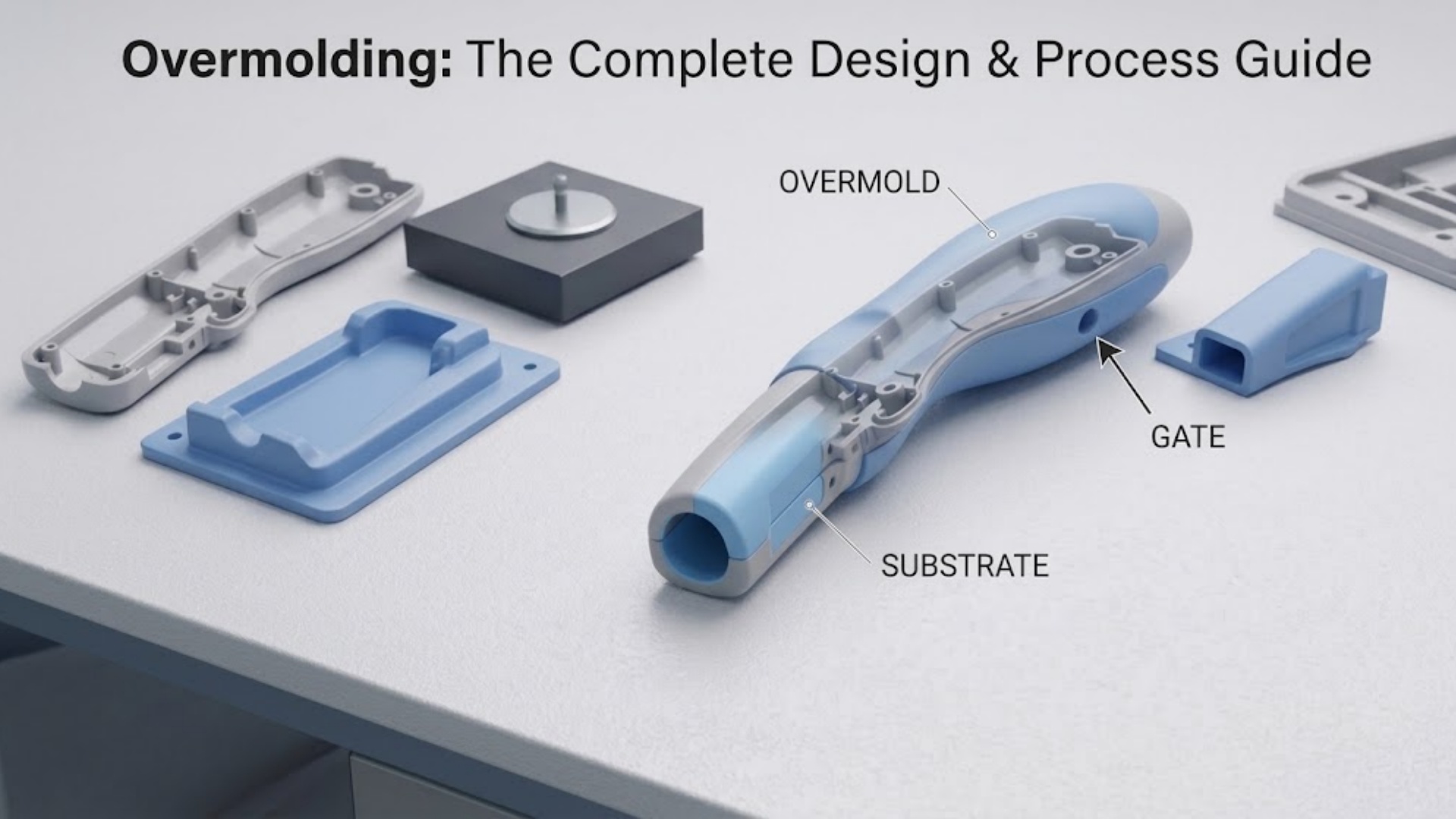
For defect avoidance on soft-touch or overmolded buttons, see overmolding defect troubleshooting. Precision mold fabrication handles the slider and lifter machining those geometries demand.
Step 4 — Tooling Strategy From EVT to Mass Production
Align tooling with program stage to control capital exposure and lead time. Hardware progresses through distinct stages, and the mold should match the volume and risk at each.
| Stage | Volume | Tooling | Notes |
|---|---|---|---|
| EVT | 1–100 parts | 3D printing / CNC / vacuum casting | Geometric fit & PCB alignment |
| DVT | 100–5,000 | Aluminum / P20 bridge tool | Real resin, mechanical/thermal validation |
| PVT / Pilot | 100s–5,000 | Bridge → hardened steel | Fast cycle trials |
| Mass Production | 10,000+ | Multi-cavity S136/H13, hot runner | Cpk control, unit economics |
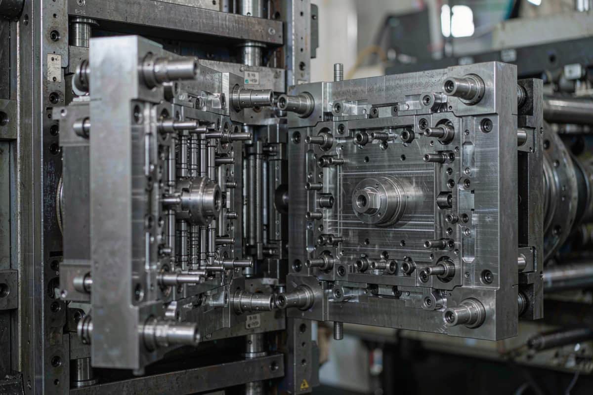
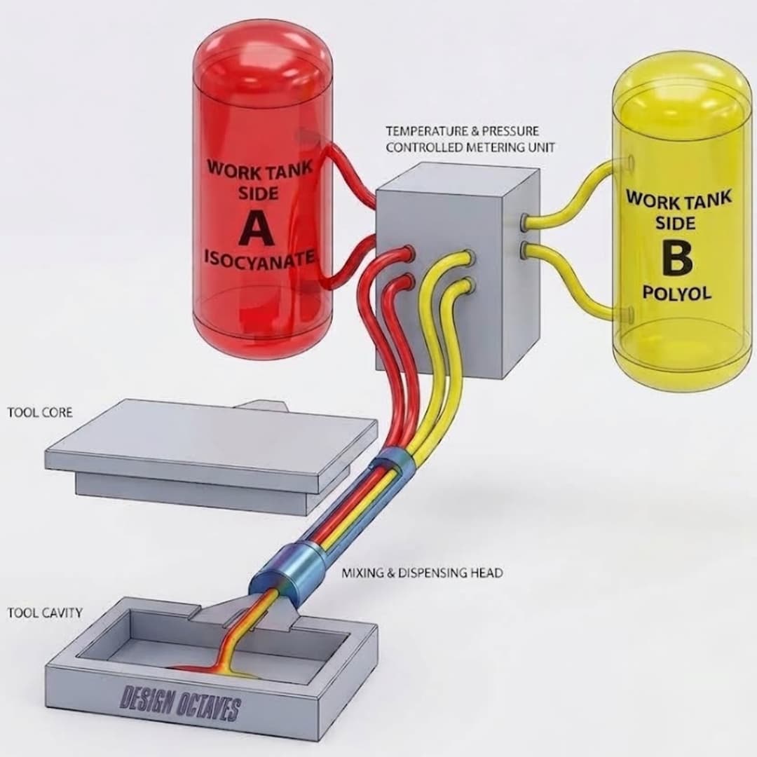
Bridge tooling delivers injection-molded parts in the intended engineering resins without the lead time of multi-cavity production tooling — ideal for DVT. For large, low-to-mid-volume housings with complex geometry, reaction injection molding (RIM) can reduce upfront tooling capital. Precision plastic mold fabrication uses hardened tool steels such as NAK80, S136, and H13; complex slides, lifters, and interchangeable inserts are typically CNC-machined to hold shutoff tolerances and prevent flash across multi-part splits. Cavity count, cold versus hot runner, and conformal cooling directly drive cycle time and unit cost.
See our precision mold fabrication and rapid prototyping services.
Step 5 — What Consumer Electronics Injection Molding Actually Costs
Cost has two parts: one-time tooling and recurring per-part. Tooling is driven by part size (more steel), complexity (side actions, hot runners), cavity count, steel grade (P20 standard / H13 high-volume / S136 corrosive resins), and surface finish (mirror polish adds cost). Per-part cost is driven by cycle time × machine hourly rate, material weight including sprue/runner, labor or automation, and yield/scrap.
Process break-even (public industry ranges, 2024–2026 — for orientation only, confirm with quote): injection molding typically becomes cheaper than CNC around 500–1,000 units for small parts; below ~1,000 units, 3D printing or CNC is often the cheaper route. A mid-complexity electronics enclosure mold commonly runs ~$6,000–$15,000 single-cavity (P20, complexity-dependent), rising to $15,000–$80,000+ for multi-cavity, hot-runner, or medical-grade tools. Per-part processing commonly lands $0.05–$0.30 for standard parts and $0.80–$2.00 where manual degating, ultrasonic welding, or printing are required. The cheapest change window is pre-steel — design-stage revisions are nearly free, while post-steel modifications cost $500–$10,000 depending on complexity. Invest in DFM before cutting steel.
Step 6 — Quality Verification and IP Protection
Quality framework. First Article Inspection (FAI) verifies 100% of critical-to-function (CTF) dimensions using CMM and optical video measurement. Process capability studies confirm critical dimensions — interlock snaps, gasket grooves — demonstrate Cpk ≥ 1.33 across multi-cavity tools. Environmental and fit testing covers drop, thermal cycling, color spectrophotometer evaluation (Delta E), and cross-hatch adhesion for coated or printed enclosures. GoodTech operates under ISO 9001, ISO 13485 (medical), ISO 14001 (environmental), and UL 746D (QMMY2) — confirm current scope on the quality system page.
IP protection. A comprehensive bilateral NDA is executed before transferring CAD, PCB STEP models, or design renders. Engineering Change Order (ECO) management keeps CAD, CAM, and physical cavities synchronized. Direct cross-border engineering support resolves DFM and material-substitution issues without stall. The dual-base structure — Chicago and Shenzhen engineering with a Vietnam site — supports a 24-hour working cadence and tariff flexibility; noted as context, not a sales claim.
How to Evaluate a Consumer Electronics Injection Molding Supplier
Use a six-criteria framework before committing:
- In-house tooling — controls quality and lead time versus third-party tooling risk.
- DFM at quote stage — does the supplier return a DFM report and mold-flow analysis, or just a price?
- Certifications — ISO 9001 baseline; ISO 13485 or IATF 16949 where applicable.
- Evidence — case studies in your product class, such as our injection molded electrical enclosure.
- Committed T1 lead time — a date, not an estimate.
- Metrology & IP — CMM capability, statistical process control (Cpk), formal ECO workflow, and NDA protocol.
FAQ
What draft angle do consumer electronics housings need? 0.5–1.5° per side on core/cavity shutoffs; add about 1° per 0.025 mm of texture depth. Deep display-window cores need the higher end.
Which plastic is best for electronic enclosures — ABS, PC, or PC/ABS? PC/ABS blend is the common default for structural housings needing UL94-V0 and drop survival; ABS for cost-sensitive handhelds; PC for impact-critical or optical-clear shells. Final choice uses the exact grade datasheet.
How much does an injection mold for an electronics enclosure cost? Industry reference: roughly $6,000–$15,000 for a mid-complexity single-cavity enclosure mold; $15,000–$80,000+ for multi-cavity, hot-runner, or medical tools. Confirm with a formal quote.
How long does tooling take from DFM sign-off to T1? Bridge molds typically 2–3 weeks; complex multi-cavity hardened-steel production molds 4–7 weeks (GoodTech reference range).
When is injection molding cheaper than CNC for electronics parts? Usually beyond about 500–1,000 units for small parts; the crossover depends on weight, complexity, and material.
How do you prevent sink marks above screw bosses on cosmetic surfaces? Core out the boss base, add gusset ribs instead of wall mass, keep the core-to-wall ratio below 60%, and apply correct pack and hold pressure.
How is EMI shielding handled with plastic enclosures? Three routes — conductive coating, conductive-filled resin, or a shield can on the PCBA. Containing emissions at the source (shield can) is the modern default for wireless products.
Contact Us
Consumer electronics injection molding succeeds when design, material, and manufacturing decisions are made together — before steel is cut. Classify the part, pick the resin by function, lock DFM rules, stage your tooling from EVT to mass production, and verify cost and supplier capability with a structured checklist.
Ready to move your enclosure from design to production? Submit your STEP files to GoodTech for a confidential DFM evaluation, material mold-flow review, and tooling proposal. Explore our full plastic injection molding capabilities.